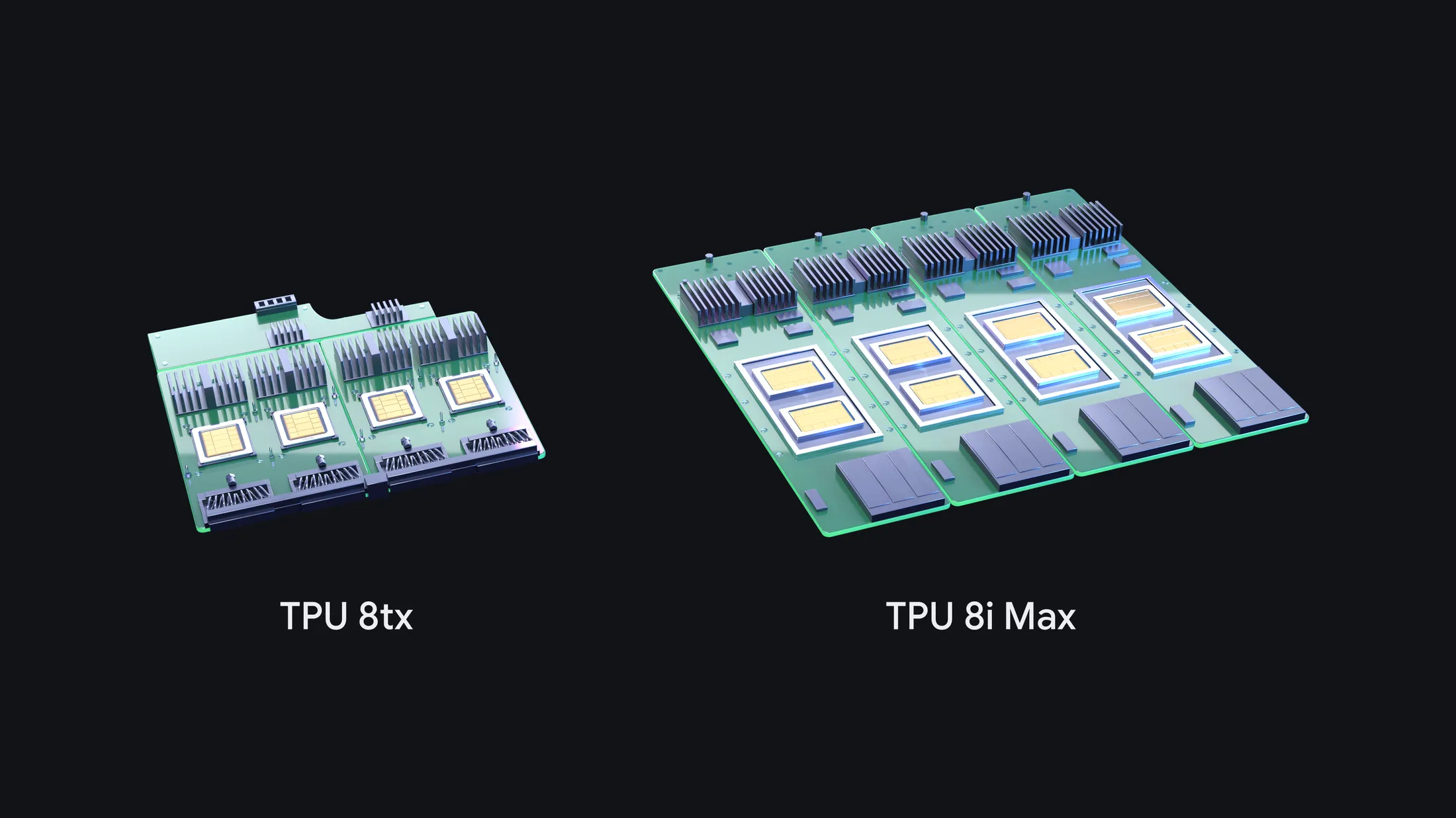
Google Cloud recently announced two additions to its eighth-generation Tensor Processing Unit lineup. TPU 8tx pairs TPU 8t silicon with 5th Generation AMD EPYC host CPUs to deliver hardware-level confidential computing for inference and small-scale training. TPU 8i Max places two TPU 8i chips in a single package (doubling compute, on-chip SRAM, and HBM bandwidth per package and fitting twice the silicon into the existing rack footprint).
Neither system uses new silicon. Google built both from the TPU 8t and TPU 8i chips announced in April, changing the packaging, host platform, and security architecture around them.
Google also disclosed that TPUs now serve nearly 100 customers, and it released software updates that include the open-source TPU Sync memory layer and general availability of Cloud Pathways and GKE dynamic slicing.
Technical Details
Google described the announcement as a “systems change,” separating a new chip, which takes years of design and manufacturing, from a new system, which rearranges compute, networking, memory, packaging, and security around an existing chip. Both products fall in the second category.
The table below places them beside the April pair:
| System | Silicon and Host | Target Workload | Disclosed Specifications |
| TPU 8t | Training ASIC with Arm Axion hosts | Large-scale training | 216 GB HBM at 6,528 GB/s, 12.6 PFLOPs FP4, 9,600-chip superpods (April disclosure) |
| TPU 8i | Inference ASIC with Arm Axion hosts and Boardfly network | Low-latency reasoning | 288 GB HBM at 8,601 GB/s, 384 MB SRAM, 10.1 PFLOPs FP4, up to 1,152 chips per pod (April disclosure) |
| TPU 8tx | TPU 8t silicon, 5th Gen AMD EPYC hosts, Boardfly network | Confidential inference and small-scale training | Up to 2x lower latency than TPU 8t with near-zero performance penalty, per Google. No absolute figures published |
| TPU 8i Max | Two TPU 8i chips in one package | Massive context windows and rack density | 2x compute, SRAM, and HBM bandwidth versus TPU 8i, per Google. HBM capacity, power, and pod size undisclosed |
TPU 8tx
TPU 8tx addresses a gap in conventional data protection. Data is encrypted at rest and in transit but must be decrypted in memory while a processor works on it. Pairing TPU 8t silicon with 5th Generation AMD EPYC hosts keeps data and model weights protected and isolated during active use.
The system also inherits the Boardfly network built for TPU 8i.
TPU 8i Max
TPU 8i Max targets the memory wall that arises when many agents coordinate. Google combined two TPU 8i chips into a single package, resulting in double the compute, SRAM, and HBM bandwidth of TPU 8i.
Because the package fits twice as much silicon within the existing rack footprint, Google delivers more compute per square foot and per watt. Applying this doubling to the April TPU 8i figures implies 768 MB of SRAM and roughly 17.2 TB/s of HBM bandwidth per package.
Software and Platform Updates
Google paired the hardware with software releases, and several are now available:
- PyTorch access: Google open-sourced TorchTPU last month, enabling PyTorch code and Hugging Face models to run natively on TPUs via the vLLM and SGLang backends. A TPU agent suite in preview integrates with Claude Code, Cursor, and Google Antigravity to automate onboarding and kernel tuning.
- TPU Sync: Google open-sourced a model-state layer that tiers KV caches across HBM, host DRAM, shared storage, and the network. Google claims more than a 90% reduction in KV transfer latency and time to first token.
- Orchestration: Cloud Pathways is generally available on GKE. GKE dynamic slicing is also generally available, and Google claims up to 5x faster job startup and 4.5x faster fault recovery.
- Agent Compute Engine: The service suspends idle agent sessions and moves working memory off the chip within milliseconds. Google does not quantify the savings.
Analysis
Google extends its modular TPU strategy with this announcement. It reuses two chip designs to ship specialized systems in months, allowing it to respond to customer requests without waiting for a new silicon cycle.
TPU 8tx moves the TPU line into regulated and government buying centers that Google has historically served with GPU-based confidential VMs, while TPU 8i Max addresses agent workloads with very large context windows.
Competitive Impact
Confidential AI compute and long-context inference have different competitive sets. In confidential computing, NVIDIA holds an established position with GPU-level confidential computing on Hopper and Blackwell, and Google itself offers Confidential G4 VMs in preview that pair NVIDIA RTX PRO 6000 Blackwell GPUs with 5th Generation AMD EPYC CPUs.
In long-context inference, TPU 8i Max competes with rack-scale GPU systems and with AWS Trainium3.
| Alternative | Model or Approach | How It Compares | Availability |
| NVIDIA Hopper and Blackwell confidential computing | GPU trusted execution environment paired with AMD SEV-SNP or Intel TDX hosts | Documented in an NVIDIA whitepaper and offered on Google Cloud. TPU 8tx protects data in use as well but has no published attestation detail | Shipping today |
| Google Confidential G4 VMs | NVIDIA RTX PRO 6000 Blackwell GPUs on 5th Gen AMD EPYC with AMD SEV | Shares the EPYC generation with TPU 8tx. TPU 8tx adds training-grade compute and the Boardfly network | Preview in all Google Cloud regions |
| NVIDIA Vera Rubin NVL72 | 72-GPU rack with NVLink and the CUDA ecosystem | Broadest software support. NAND Research’s April note put aggregate memory near 20 TB per rack, against an undisclosed TPU 8i Max capacity | Expected 2H 2026 on Google Cloud, per April note |
| AWS Trainium3 | Unified ASIC with 144 GB HBM3e at 4.9 TB/s per chip, 144-chip UltraServer | TPU 8i delivers 8,601 GB/s per chip and TPU 8i Max doubles it per package. The sources reviewed for this note do not cover an equivalent AWS confidential option on Trainium | Generally available since December 2025 |
Google’s differentiation is strongest where the integrated stack matters. No other accelerator vendor ships a single system that runs confidential inference, private fine-tuning, and reinforcement learning on a fast, low-latency network. TPU 8i Max packs more silicon per rack than the TPU 8i it extends.
Final Thoughts
Google has turned a modular design philosophy into a product cadence. Four systems built from two chips in a single year provide a concrete answer for regulated buyers and for teams running agents with million-token contexts. The open-source TorchTPU and TPU Sync releases lower the cost of trying TPUs.
Customers evaluating confidential AI infrastructure and long-context inference for 2027 now have a Google option that combines training-grade compute with hardware isolation.