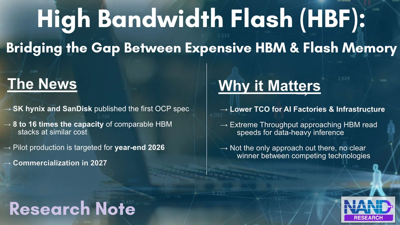
At the recent FMS 2026, SK hynix and SanDisk announced the first open technical specification for High Bandwidth Flash (HBF), formalizing a new memory category that sits between high-bandwidth memory (HBM) and solid-state drives.
The specification, released through the Open Compute Project, defines packages with up to 512GB of capacity, using 8-high and 16-high NAND die stacks connected to processors via UCIe, the open chiplet interconnect standard, with three bandwidth grades spanning roughly 0.4TB/s to 3.0TB/s.
The motivation for HBF is that HBM has hit a capacity and cost ceiling, and AI inference workloads are outgrowing it faster than the memory industry can scale it. Top-tier HBM stacks on NVIDIA H200 and B200 accelerators cap out at 141GB and 192GB, respectively, while LLM deployments increasingly require hundreds of gigabytes to over a terabyte of fast memory per node to hold model weights and a key-value cache simultaneously.
HBM costs roughly $20 to $30 per gigabyte, making terabyte-scale in-package memory economically prohibitive at current prices. HBF targets that gap with NAND-based stacks that could deliver 8 to 16 times the capacity of a comparable HBM stack at a similar cost.
Interestingly, while Google and Tenstorrent joined SK hynix and SanDisk as founding members of the HBF consortium, NVIDIA, AMD, Intel, Broadcom, Marvell, Micron, Samsung, Qualcomm, and Western Digital have not.
This (currently) leaves the standard unsupported by merchant GPU vendors, which would need to adopt it for HBF to reach mainstream AI infrastructure.
Technology Overview
HBF adapts the die-stacking approach that made HBM successful, but replaces DRAM with NAND flash and repositions the resulting memory as a capacity-oriented companion to HBM rather than a replacement.
SanDisk‘s contribution is CMOS-Bonded-to-Array technology, which bonds logic and NAND arrays directly rather than routing them through a traditional array-on-periphery layout. SanDisk says this construction materially increases achievable I/O density and bandwidth per stack.
The first-generation specification targets read-mostly, capacity-bound data such as model weights, rather than the low-latency read-and-write cycling that transformer inference performs on the KV cache.
Highlights include:
- Capacity and stacking: 8-high and 16-high NAND die stacks, up to 512GB per package, with first-generation dies each packing 256Gb
- Bandwidth grades: three tiers ranging from roughly 0.4TB/s to 3.0TB/s for the highest grade, delivered via UCIe rather than a proprietary interposer link
- Generational roadmap: SK hynix and SanDisk have outlined Gen 2 and Gen 3 targets exceeding 2TB/s and 3.2TB/s of read bandwidth, respectively, with stack capacity rising to 1TB and 1.5TB
- Endurance and access pattern: because HBF is flash rather than DRAM, it has write endurance limits and higher write latency than HBM, restricting near-term use to read-dominated workloads
- Performance claim: SK hynix’s H³ simulation, pairing eight HBM3E stacks with eight HBF stacks on an Nvidia B200-class platform, delivered up to 2.69 times higher throughput per watt than an HBM-only configuration; independent validation of this figure has not been published
The architecture assumes HBM and HBF coexist on the same package or module, with HBM handling latency-sensitive key-value cache traffic and HBF handling the larger, more static footprint of model weights.
Analysis
SK hynix and SanDisk present HBF as an open, standards-based solution to the AI memory wall, in contrast to Samsung’s proprietary zHBM concept, which stacks HBM directly atop the accelerator (rather than introducing a new flash tier). The split forces AI infrastructure buyers and accelerator designers to choose an architecture before either camp has shipped production silicon.
Kioxia has staked out a third position, extending HBM through a PCIe 6.0 SSD tier, the GP1 series, that reaches 10 million IOPS without requiring a new die-stacking standard or interconnect adoption.
- Open standard versus proprietary stack: HBF’s OCP specification and UCIe interconnect let multiple NAND and accelerator vendors interoperate, while Samsung’s zHBM remains a single-vendor concept without a published open specification
- Consortium risk: an open standard has limited value without the accelerator vendors that dominate AI compute; the absence of Nvidia and AMD from the HBF consortium is the clearest constraint on how quickly the standard could reach volume deployment
- Kioxia’s lower-risk path: by building on the existing PCIe SSD ecosystem rather than a new memory class, Kioxia can ship evaluation units by the end of 2026, ahead of HBF’s 2027 commercialization target, though at lower bandwidth per byte than in-package HBF
Practitioner Impact
AI accelerator designers and hyperscale infrastructure teams are the primary near-term audience for HBF, not enterprise IT buyers. Adopting HBF requires accelerator vendors to design UCIe-compatible chiplet packaging around it, a multi-year silicon decision, and model-serving software to route weight storage and KV cache traffic to the correct memory tier.
Additionally:
- Packaging and integration: HBF must be designed into the accelerator package at tape-out, so practitioners cannot retrofit it onto existing GPU generations already in production
- Software and scheduling: inference runtimes need memory-tiering logic that places weights on HBF and active cache on HBM, adding a layer of memory management that most current serving stacks do not implement
- Availability timeline: SK hynix and SanDisk expect a pilot production line to be operational by the end of 2026, with commercialization targeted for 2027. Therefore, practitioners evaluating HBF today are planning for next-generation platforms, not current deployments.
Competitive Impact
HBF competes with three distinct approaches to the same underlying problem. Each alternative trades bandwidth, latency, capacity, cost, or time-to-market differently, and none has established itself as the default architecture:
| Alternative | Model / Approach | How It Compares to HBF |
| HBM3E / HBM4 | DRAM stacked directly on or adjacent to the accelerator package | Higher bandwidth per stack and full read/write performance, but capped near 141-192GB per accelerator and priced at roughly $20-30 per gigabyte, an order of magnitude above projected HBF economics |
| CXL memory pooling (Marvell Structera, Astera Labs Leo, XConn) | DRAM pooled across multiple server hosts through a CXL switch | Solves server-level memory capacity rather than per-accelerator weight storage; round-trip latency near 460 nanoseconds is well above on-package HBF access, and pooling operates at the rack level, not the chiplet level |
| Kioxia GP1 (PCIe 6.0 SSD) | NAND SSD accessed over PCIe with GPU Direct Storage | Requires no new packaging standard and is shipping evaluation units in 2026, but bandwidth is bound by the PCIe link rather than an in-package interconnect, giving it lower peak throughput than HBF’s UCIe-based design |
| Samsung zHBM | HBM stacked vertically atop the AI accelerator | Targets the same near-compute position as HBF but stays DRAM-based, retaining HBM’s cost structure while improving bandwidth and thermal performance rather than adding a distinct capacity tier |
HBF’s differentiation is strongest on the capacity-per-dollar argument relative to HBM and on interconnect openness relative to Samsung‘s proprietary path.
Its differentiation is weakest on timing and ecosystem breadth. Kioxia‘s SSD-based approach can reach customers sooner with lower architectural risk, and HBF still lacks commitment from the two accelerator vendors, NVIDIA and AMD, which control the vast majority of AI training and inference deployments.
Final Thoughts
HBF is a credible technical answer to a real problem. There’s little question that AI inference is running out of affordable memory capacity faster than HBM roadmaps can keep pace. The economics, roughly 8 to 16 times the capacity of HBM at comparable cost, are compelling enough to explain why Google and Tenstorrent signed on early.
What remains unresolved is adoption outside that small founding group. A memory standard’s value scales with the number of accelerator platforms that support it, and the absence of NVIDIA, AMD, Intel and Broadcom from the consortium means HBF’s near-term addressable market is limited to whichever silicon Google, Tenstorrent, and any future joiners build around it.
Samsung‘s competing zHBM concept and Kioxia‘s SSD-based GP1 series both suggest that the rest of the industry is not yet convinced that HBF is the correct architecture, even as everyone agrees the underlying capacity problem is real.
The next twelve months, covering the pilot production line SK hynix and SanDisk expect by year-end and the 2027 commercialization target, will determine whether HBF becomes the industry’s shared answer to the AI memory wall or one of several competing tiers that data center architects must choose among on a platform-by-platform basis.