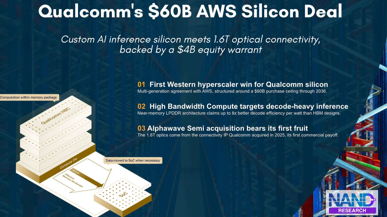
Qualcomm and Amazon Web Services announced a multi-generation agreement covering custom AI inference silicon and 1.6T optical connectivity for AWS data centers. The deal is structured around a warrant for up to 25 million Qualcomm shares at $161.26 per share, vesting as AWS meets purchase milestones, with a $60 billion ceiling on silicon and connectivity purchases through 2036.
The agreement gives Qualcomm its first Western hyperscaler customer for data center silicon, addressing decode-heavy AI inference workloads with a memory-capacity-optimized architecture Qualcomm calls High Bandwidth Compute.
It also marks the first commercial validation of the connectivity technology Qualcomm acquired in its 2025 purchase of Alphawave Semi, which supplies the SerDes and optical DSP building blocks for the 1.6T optics component of the deal.
The announcement matters because it extends the custom silicon trend already established at Google and Meta to a third major hyperscaler, and because it gives Qualcomm a second data center revenue stream, combining silicon and connectivity, built largely from a single acquisition in a single year.
Details
The agreement covers two distinct product lines that Qualcomm and AWS will co-develop across multiple generations:
- Compute: a custom AI inference chip
- Connectivity: a 1.6 terabit optical networking infrastructure built on technology Qualcomm acquired through Alphawave Semi.
The compute component is built around Qualcomm’s unique High Bandwidth Compute architecture, first disclosed alongside Qualcomm’s AI200 and AI250 accelerator cards. HBC stacks LPDDR memory dies in a 3D package directly above a compute die, rather than placing memory on a separate substrate connected via an interposer, as HBM does.
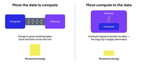
Placing the memory this close to the compute logic shortens the physical data path and enables a meaningful share of memory-access work to happen on-die, which underpins Qualcomm’s bandwidth and efficiency claims.
The approach trades the raw per-stack bandwidth of HBM4, roughly 3.3 TB/s per stack in current designs, for a much larger pool of lower-cost, lower-power LPDDR capacity, stacked closer to the compute engine:
- HBC Gen 1 performance of up to 133 TB/s of aggregate bandwidth and up to 768GB of stacked memory capacity per accelerator card, with the first commercial shipment expected around mid-2027 as part of the AI250 card (independent of this AWS deal).
- 4-8x better decode performance per watt and 5-7x better bandwidth per watt versus HBM-based accelerator designs for larger batch sizes, rising to as much as 200x on mixed small-and-large batch workloads such as coding assistants.
- The architecture targets memory-capacity-bound decode inference, specifically the token-by-token generation phase of a large language model response, where maintaining a large key-value cache in memory matters more than peak compute throughput.
- 1.6T optical connectivity modules built on Alphawave’s SerDes and optical DSP IP, expected to link AWS’s custom silicon and networking infrastructure at higher throughput than current-generation interconnects.
- Qualcomm and AWS describe the collaboration as spanning multiple future generations of silicon and connectivity.
Custom silicon revenue under the AWS agreement is expected to begin in Qualcomm’s fiscal Q1 2027.
Analysis
The deal is the latest evidence that the data center component of Qualcomm’s diversification strategy is entering its revenue phase. Qualcomm has spent recent quarters building a data center narrative focused on AI inference and connectivity as part of a broader push beyond its smartphone core into automotive, IoT, and data center silicon.
The company used its June 2026 investor day to lay out a multi-year data center strategy with defined inflection points over the next three to five years.
The AWS agreement is the first hyperscaler contract with disclosed financial scale to back that narrative, joining a growing list of data center customer relationships Qualcomm has disclosed over the past year:
- Unnamed Hyperscaler: During its April 2026 earnings call, Qualcomm CEO Cristiano Amon disclosed a multi-generation custom silicon engagement with an unnamed hyperscaler, with initial chip shipments targeted for December 2026, a timeline that closely aligns with the Q1 fiscal 2027 revenue start now disclosed for AWS. It’s unclear whether the two engagements involve the same customer.
- Meta: At its June 2026 investor day, Qualcomm named Meta as a data center CPU customer under a separate multi-generation agreement. The product line is distinct from the AI200/AI250 inference accelerators and the AWS silicon.
- HUMAIN: Qualcomm’s first named data center infrastructure customer was HUMAIN, the Saudi Arabian AI enterprise, which, in October 2025, committed to deploying 200 megawatts of Qualcomm AI200 and AI250 rack-scale systems starting in 2026.
The deal also marks the first commercial payoff from Qualcomm’s $2.4 billion acquisition of Alphawave Semi, completed in 2025 to secure high-speed connectivity and chiplet IP for data center use. The optics component of the AWS deal draws directly on that acquired technology.
Structuring the agreement as an equity warrant tied to purchase milestones aligns AWS’s financial upside with actual procurement volume, giving Qualcomm a built-in incentive for AWS to meet purchase thresholds that a standard purchase order would not provide.
Qualcomm has also attached specific public targets to this diversification push. At the June 2026 investor day, the company raised its fiscal 2029 non-handset revenue target to roughly $40 billion, up from a prior $22 billion goal, and gave a first-ever data center revenue target of more than $15 billion by fiscal 2029, a business it has described as generating almost no revenue today.
Qualcomm paired that with a $10 billion fiscal 2029 automotive revenue target, backed by a roughly $65 billion automotive design-win pipeline.
The AWS agreement is the largest single data point disclosed so far toward the $15 billion data center goal, though Qualcomm has not broken out how much of the $60 billion AWS purchase ceiling would count toward fiscal 2029 revenue specifically, since the agreement runs through 2036.
The technical substance of the deal is real. The HBC architecture and the Alphawave-derived optics are working silicon and IP, and the warrant structure shows that AWS has enough conviction in the roadmap to accept vesting tied to future purchases.
Reaching the $15 billion fiscal 2029 data center target depends on Qualcomm converting its current mix of named and unnamed engagements, including AWS, Meta, HUMAIN, and the April hyperscaler, into recurring, at-scale silicon volume rather than one-time design wins.
Competitive Landscape
Qualcomm enters the custom silicon market, already occupied by Broadcom, Marvell, and MediaTek, each with established hyperscaler relationships built over several product generations. The AWS deal gives Qualcomm its first foothold in that market, but it enters a narrower segment than its more established rivals
| Alternative | Model / Approach | Relative to the Qualcomm-AWS |
| Marvell (AWS Trainium/Inferentia) | Co-design partner embedded inside AWS’s captive accelerator programs, spanning both training and inference SoCs. | Serves a different tier of AWS’s silicon portfolio. Trainium and Inferentia are AWS’s own branded accelerators; Qualcomm’s chips are a separate, externally branded inference option AWS is adding alongside them. |
| Broadcom (Google TPU, Meta MTIA) | Dominant ASIC co-design partner for Google‘s TPU line and Meta‘s MTIA, with the deepest revenue base in custom hyperscale silicon. | Far larger in booked revenue and design tenure. Qualcomm’s AWS win validates the category Broadcom already leads, and Broadcom’s own Google and Meta relationships remain intact. |
| MediaTek (Google TPU v9) | Second-source design partner on Google’s TPU roadmap, expanding its data center ASIC unit alongside its core smartphone business. | A comparable diversification move by a mobile-silicon vendor into hyperscale ASICs. MediaTek’s design win sits with Google’s TPU program, and it carries no equivalent connectivity or optics component. |
| NVIDIA (GPU inference) | General-purpose GPU platform (Blackwell, Rubin) with the largest share of both training and inference workloads and the deepest software ecosystem. | Broader and more flexible across workload types. Qualcomm targets a narrower slice, memory-capacity-bound decode inference, where LPDDR-based architectures claim an efficiency edge over HBM-based GPUs. |
| AMD (Instinct MI350X) | HBM3e-based accelerator (288GB) competing directly for inference workloads across multiple hyperscalers. | Optimized for memory bandwidth and general inference throughput. Qualcomm’s HBC design trades bandwidth headroom for lower power and cost per token on decode-heavy workloads. |
Qualcomm’s strongest differentiation is its pairing of custom compute with the connectivity IP it acquired through Alphawave Semi, a combination none of Marvell, Broadcom, or MediaTek currently offers as a single integrated deal with the same hyperscaler.
Marvell’s existing role inside AWS’s own Trainium and Inferentia programs is a separate, incumbent relationship; Qualcomm is competing for a distinct, additional slice of AWS’s silicon spend alongside it.
Final Thoughts
Qualcomm’s AWS agreement gives the company its first Western hyperscaler customer for data center silicon and turns the Alphawave Semi acquisition into a revenue-generating asset within twelve months of closing.
The warrant structure, the multi-generation framing, and the pairing of compute with 1.6T optical connectivity all point to a decade-long purchasing relationship spanning multiple silicon generations.
The deal’s significance lies more in Qualcomm’s strategic trajectory than in near-term revenue. Qualcomm has turned its stated diversification ambition into a signed agreement with a top-three hyperscaler, backed by acquired technology that is already bearing commercial fruit. That combination gives its data center strategy the credibility it lacked a year ago.
This is a big win for Qualcomm, strongly validating both its technology and diversification strategy.