First-generation silicon shows Dragonfly AI250 on track for 2027 sampling
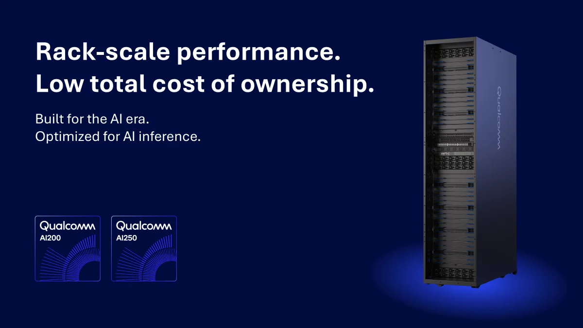
Qualcomm has validated first-generation High Bandwidth Compute (HBC) silicon, providing the Dragonfly AI250 inference accelerator with its first hardware proof point. The company reports 18x the effective memory bandwidth of LPDDR5X and more than 5x the bandwidth per watt compared with projected HBM4 specifications.
Four months after HBC debuted at Qualcomm’s June Investor Day, it has progressed from slide to working silicon. With AI250 sampling set for the first half of 2027, this marks the most important technical checkpoint Qualcomm has cleared in its data center push.
Let’s look at how HBC works, why an inference accelerator needs it, what the validation results showed, and the milestones behind it.
What is HBC?
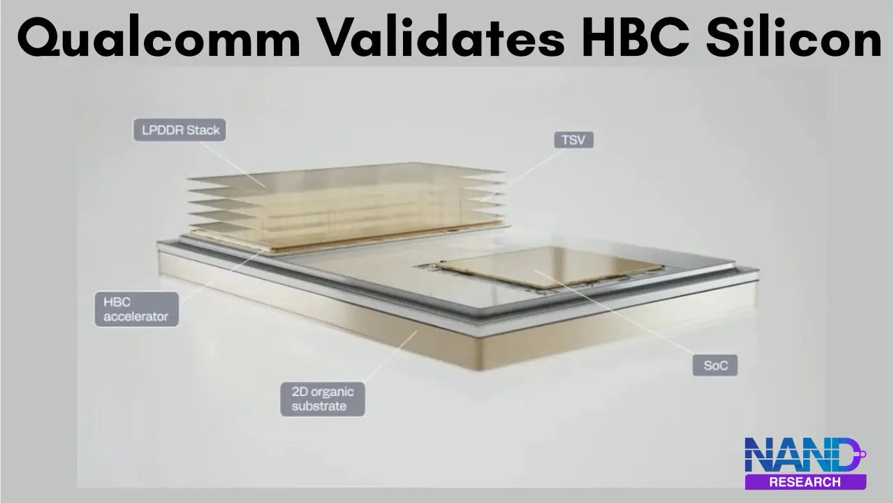
HBC is a near-memory compute architecture that stacks LPDDR DRAM dies over an active AI accelerator base die. Through-silicon vias (TSVs) connect the DRAM layers to the compute logic beneath, and Qualcomm builds the stack using direct wafer-to-wafer bonding.
Traditional AI accelerators place HBM stacks beside the compute die on an expensive silicon interposer. HBC places the compute die beneath the memory.
The base die is not a full processor. It handles the most memory-bandwidth-intensive operations near the DRAM and sends the results to the larger compute die at the center of the accelerator.
Data travels micrometers within the stack, where an HBM design moves it millimeters between the stack and the GPU package. Qualcomm describes the design as near-memory compute and distinguishes it from compute-in-memory approaches.
Three properties define the design:
- LPDDR as the memory: Qualcomm uses LPDDR5X, which offers higher capacity per stack at lower power than HBM and relies on a mature supply chain.
- Standard packaging: Multiple HBC stacks can be integrated into a single device without a 2.5D interposer such as CoWoS, eliminating a costly and supply-constrained step.
- Compute in the stack: HBC provides real compute under the DRAM, which is why Qualcomm calls it high-bandwidth compute and does not market it as a memory product.
Why does an AI Accelerator needs HBC?
Inference is a memory problem. Every token a model generates requires the accelerator to pull model data through its compute units, so memory bandwidth and the energy spent moving data set throughput, power draw, and total cost of ownership.
Compute capability has risen sharply over the past decade, while memory bandwidth has grown far more slowly. That gap is the memory wall, and agentic AI workloads, with their long contexts and continuous inference, push against it harder than any prior workloads.
HBM is the standard answer, and it carries costs that grow with every cluster:
- Power: Moving data off-package over millimeters consumes energy, which raises the cost of every token.
- Packaging: HBM relies on 2.5D interposers such as CoWoS, which are both expensive and supply-constrained.
- Capacity: A single HBM stack holds roughly 32 to 64 GB, limiting how much model and context can fit near the compute.
- Supply: HBM remains tight, and the entire semiconductor supply chain is operating at full capacity, with shortages and price increases across wafers, assembly, and test.
HBC attacks all four at once. Stacking LPDDR on compute delivers SRAM-like proximity with DRAM-class capacity, providing 6x the bandwidth per watt of HBM and 200x the capacity per watt of on-chip SRAM. The capacity of an HBC stack is also intended to exceed current HBM4 implementations.
The architecture gives Qualcomm a credible path into inference infrastructure without competing with Nvidia and AMD on raw compute, and it plays to Qualcomm’s strengths in low-power design and TSV packaging expertise built over decades of smartphone silicon.
HBC also trades peak HBM bandwidth for capacity and efficiency, and its bandwidth figures are effective numbers that depend on the base die doing work inside the stack.
Qualcomm’s HBC Silicon Validation
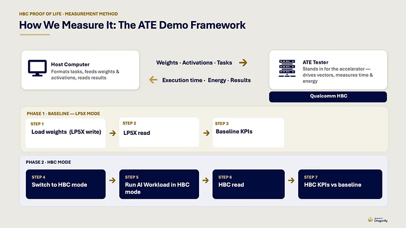
Qualcomm’s announcement confirms that first-generation HBC functions as designed in hardware. The lab validated the end-to-end memory read-write path and near-memory computation at production-representative dimensions.
Engineers connected an early HBC sample stack to industry-standard automated test equipment, ran randomized weights and activations through it, and measured the stack both as an LPDDR5X device and as an HBC device.
The test stack had two DRAM layers, and validation included thermal investigations.
| Measure | Result | Compared against |
| Effective memory bandwidth | 18x | LPDDR5X implementations |
| Bandwidth per watt | More than 5x | Projected HBM4 specifications |
| AI250 card bandwidth | 133 TB/s effective | AI200 with LPDDR5X |
The 18x gain matches the figure Qualcomm gave at Investor Day, so the silicon delivered on the roadmap’s bandwidth promise. The efficiency result came in slightly below the 6x bandwidth-per-watt target Qualcomm articulated in June. The 133 TB/s figure represents the total effective bandwidth of the AI250 card and does not apply to a single HBC module.
The validation also supports the manufacturing story. Qualcomm says its Dragonfly AI250 data center AI accelerator, built on HBC, has already taped out. The results should dispel doubts about the AI250’s high-yield manufacturing next year.
Milestones on the Path to Production
Qualcomm has reported steady progress on HBC since June, and each milestone added a different kind of evidence:
| Date | Milestone | Detail |
| Nov 2, 2026 | Gen 1 silicon validated | San Diego lab validation of the full read-write path and near-memory compute, with 18x effective bandwidth over LPDDR5X and over 5x bandwidth per watt against projected HBM4. |
| Sep 23, 2026 | HBC extends to client devices | At Snapdragon Summit, CEO Cristiano Amon described HBC as a coprocessor for Snapdragon, with PCs, smart glasses, and vehicles to follow and details due at MWC Barcelona in March 2027. |
| Aug 26, 2026 | Memory partners engaged | At the Deutsche Bank conference, EVP Durga Malladi said he went to Korea after Investor Day to meet two major memory makers. The Elec reports Samsung and SK hynix are developing HBC alongside their HBM roadmaps, with TSMC eyed for integration. |
| Jul 29, 2026 | First HBC chip taped out | Qualcomm told investors on its fiscal Q3 call that the first-generation HBC chip had taped out, setting up a mid-2027 launch. |
| Jun 24, 2026 | HBC unveiled | Investor Day debut under the Dragonfly brand, with a roadmap from Gen 1 in the AI250 to Gen 2 in the AI300, plus a forecast of $15 billion in data center chip sales by fiscal 2029. |
The customer picture strengthened alongside the technology. Qualcomm disclosed Meta as a customer during its Investor Day, and reports suggest Microsoft Azure plans to deploy HBC on the AI250 and AI300.
Two milestones remain on the published roadmap:
- Qualcomm will sample the AI250, the first accelerator with HBC Gen 1, in the first half of 2027.
- AI300 follows in 2028 with second-generation HBC and a claimed 54x the bandwidth of the AI200.
Analyst’s Take
Qualcomm’s HGC validation shows stacked LPDDR over an active base die works in silicon, the bandwidth multiplier holds, and the energy efficiency lands at more than 5x against a 6x target. It’s a critical step toward Qualcomm’s data center ambitions.
Qualcomm reports fiscal fourth-quarter results on November 4 after the market closes. Pacific. Expect the data center story to share the stage with Apple modem headwinds and handset weakness, and watch for any update on AI250 timing, customer commitments, and the Samsung and SK hynix work.