IBM and the U.S. Department of Commerce announced a Letter of Intent to establish Anderon, a standalone company that will operate the United States’ first pure-play quantum chip foundry.
The initiative has a combined commitment of $2 billion, including $1 billion in proposed CHIPS Act R&D incentives from the Department of Commerce and $1 billion in cash from IBM, supplemented by IBM’s intellectual property, fabrication assets, and an existing skilled workforce.
Anderon will be headquartered in Albany, New York, where IBM has operated semiconductor research and fabrication facilities for more than two decades.
Details
IBM’s core technical proposition with Anderton is the application of mature 300mm semiconductor wafer manufacturing disciplines to quantum processor fabrication, a domain that has until now operated largely at research scale.
The 300mm format is the same wafer size used in leading classical semiconductor fabs, and its adoption for quantum hardware brings process automation, tool availability, and throughput assumptions from the classical world into the quantum domain.
IBM’s shift to this format at Albany in late 2025 produced the Nighthawk and Loon processors, both of which are now in active production under these conditions.
Technical Capabilities
The technical scope of announced capabilities spans several quantum processor manufacturing domains:
- 300mm superconducting qubit wafer fabrication: covers the base process flows for superconducting qubit and supporting electronics wafers, with plans to expand into additional quantum modalities over time
- Superconducting wiring processes: supports the interconnect layers required for qubit coupling and readout
- Through-silicon vias (TSVs) enabling 3D integration: a capability relevant to multi-chip qubit stacking architectures
- Bump interconnect technology: enables flip-chip assembly of quantum processors with classical control electronics
- Dedicated process design kits (PDKs): provides a defined starting point for external customers to design quantum chips against qualified process layers (analogous to PDK structures in classical foundry services)
- Integrated In-line wafer testing and metrology: enables rapid defect identification and process refinement without waiting for end-of-line test results
- Established baseline fabrication routes: reduces per-cycle iteration time, enabling parallel development of multiple processor architectures simultaneously
IBM says that moving to 300mm production at Albany in late 2025 halved the time required to build each processor generation and increased the physical complexity achievable per chip by a factor of ten. These gains reflect process automation, tool density, and parallelism available at the 300mm scale rather than any fundamental change to the underlying qubit physics.
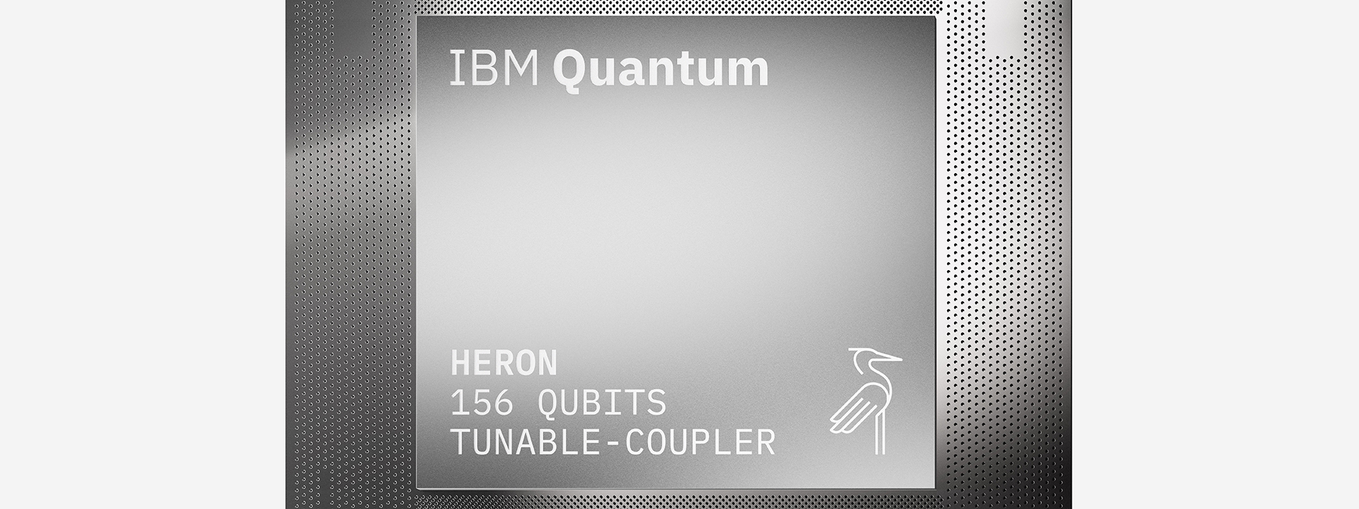
The Nighthawk processor, IBM’s current production chip with 120 qubits and 218 tunable couplers, and the experimental Loon processor, which demonstrates fault-tolerant component architectures with six-way qubit connectivity, were both fabricated in Albany.
IBM’s CHIPS R&D award is the largest single allocation from a broader $2.013 billion federal quantum portfolio, which the Department of Commerce distributed among nine companies. Other recipients include GlobalFoundries ($375 million), D-Wave Quantum, Rigetti Computing, Infleqtion, Atom Computing, PsiQuantum, and Quantinuum (each receiving $100 million), and Diraq ($38 million).
The differential between IBM’s $1 billion award and those of all other recipients demonstrates the federal government’s bet on manufacturing infrastructure as the lever for U.S. quantum leadership.
Analysis
The IBM quantum program has maintained a consistent roadmap: quantum advantage by the end of 2026, fault-tolerant quantum computing by 2029. The transition to 300mm fabrication at Albany, which IBM formalizes and scales, gives that roadmap a credible manufacturing foundation.
Practitioners evaluating IBM as a long-term quantum platform partner now have evidence that the company’s hardware delivery commitments rest on an industrialized fabrication process rather than artisanal chip production, a distinction that is material when scoping multi-year enterprise quantum programs.
For practitioners at organizations building quantum applications on IBM’s platform, the key near-term implications include:
- Faster processor iteration cycles: IBM’s halved chip development timeline at Albany accelerates the delivery cadence for new Nighthawk generations, with gate depth targets increasing from 5,000 two-qubit gates today to 7,500 by the end of 2026 and 10,000 in 2027
- Reduced fabrication variability: 300mm production automation and in-line metrology reduce lot-to-lot variation in qubit characteristics, which directly affects circuit fidelity and error correction overhead
- A clearer path to fault-tolerant systems: IBM’s fabrication infrastructure provides the substrate on which IBM’s Loon and successor fault-tolerant architectures will be built toward the 2029 FTQC target
- Supply chain security: a domestic U.S. fabrication capability removes geopolitical risk from the quantum hardware supply chain, a consideration relevant to government and regulated-industry quantum programs
IBM’s Anderon quantum manufacturing initiative extends the company’s position in quantum computing across multiple vectors.
Regional Benefit
IBM has a long manufacturing legacy in the Hudson Valley, spanning more than a century. Its semiconductor research at Albany NanoTech runs over 20 years, during which IBM and its partners have produced landmark process advances, including nanosheet transistor technology, the world’s first 2nm node demonstration, and now the first production-scale quantum wafer fabrication on 300mm format.
The Albany complex is already staffed with quantum fabrication engineers, already equipped with the relevant tooling, and already running production for IBM’s own processors. Anderon does not build from scratch; it scales an operating platform.
Supply Chain
The supply chain is among the most structurally significant aspects of the announcement. Quantum hardware currently lacks an equivalent to the classical semiconductor supply chain: no standardized wafer formats in broad use, no third-party foundry services calibrated to quantum process requirements, and no ecosystem of specialized materials and component suppliers at scale.
By establishing 300mm quantum wafer production with defined PDKs and in-line characterization, IBM creates the conditions for a supply chain to form around it.
Equipment suppliers, materials companies, and calibration services can invest in quantum-specific product development against a known production platform rather than a fragmented research landscape.
This supply chain formation effect reinforces IBM’s central position in quantum hardware manufacturing for years beyond the period during which any specific processor generation holds a performance advantage.
Competitive Landscape
The competitive implications of the move differ significantly by category of quantum company. IBM’s initial process scope is superconducting qubits, and its foundry value proposition only applies to companies working in that domain:
- Trapped-ion players like IonQ and Quantinuum operate architectures with no silicon wafer process commonality with superconducting fabrication, so IBM’s services do not address their manufacturing needs.
- Microsoft‘s topological qubit program, built around Majorana 1 and distinct fabrication processes, is similarly orthogonal.
| Company | Architecture | Fab Approach | Impact to IBM |
| Google Quantum AI | Superconducting (Willow, 105 qubits) | In-house, Santa Barbara facility | Minimal; unlikely to outsource to a competitor |
| Microsoft | Topological (Majorana 1) | Proprietary; distinct process from superconducting silicon | None; incompatible architecture |
| IonQ / Quantinuum | Trapped ion | No silicon wafer commonality with superconducting process | None in current scope |
| Rigetti / IQM / SEEQC | Superconducting (various) | Captive or small-batch; no 300mm access | Potential customers; IP risk is key adoption barrier |
| SkyWater Technology | Multi-architecture foundry services | 200mm CMOS; government-program focused | Direct competitor for government quantum fab contracts |
Within the superconducting segment, IBM faces a real commercial question. Rigetti, IQM, and SEEQC are the most plausible customers, as they share IBM’s basic process architecture and currently lack access to 300mm fabrication. However, each of these companies competes directly with IBM in the quantum system and services markets.
SkyWater Technology is Anderon’s most direct foundry services competitor in the US quantum segment, operating a 200mm CMOS foundry oriented toward government-program custom fabrication (the same environment where early IBM quantum chips were developed at its Yorktown Heights facility).
Its 300mm capability and process depth give IBM/Anderon’s a technical edge in throughput and complexity, but SkyWater’s government relationships and its non-competitor positioning relative to quantum hardware makers are genuine differentiators for customers who prioritize process IP neutrality.
Globally, no equivalent quantum foundry exists. China’s quantum hardware programs are advanced in research but lack IBM’s investment in manufacturing infrastructure. Japan’s Rapidus, focused on classical 2nm production, does not address quantum wafer requirements.
Anderon will operate without a direct international peer in the 300mm quantum foundry market in the near- to mid-term.
Final Thoughts
The Anderon announcement reinforces IBM’s hardware roadmap execution by formalizing 300mm wafer production capabilities already demonstrated in production and creating a potential platform business that generates value from the broader quantum ecosystem (not just from IBM’s own systems).
The combined $2 billion commitment, the largest single quantum manufacturing investment in US history, reflects both the federal government’s stake in domestic quantum supply chain independence and IBM’s confidence in its fabrication differentiation as a durable competitive advantage.
The Albany NanoTech regional ecosystem gives IBM/Anderon a concrete advantage that matters at this stage of the quantum industry’s development. IBM’s 20-plus years of semiconductor research in Albany, the established equipment infrastructure, the quantum fabrication team already operating Nighthawk and Loon in production, and the surrounding Tech Valley supply chain and workforce pipeline substantially reduce IBM’s risk.
The biggest open question is the extent of commercial adoption by external quantum hardware companies, specifically whether Anderon’s superconducting competitors will use IBM’s foundry despite the inherent IP exposure risk.
IBM compared its efforts in quantum fabrication to TSMC’s semiconductor capabilities. While the analogy holds up structurally, TSMC succeeded in part because its customer base included companies with no systems business in common with TSMC.
IBM’s Anderon doesn’t have that luxury in the superconducting segment. IBM’s answer, whether through governance structure, process-isolation architecture, or external investor dilution of IBM’s controlling interest, will determine whether Anderon becomes a quantum industry platform or a well-funded captive fab.
What is not in question is that IBM, through the combination of the Albany NanoTech investment history and the Anderon commitment, now holds the most advanced quantum wafer fabrication capability in the United States.
This will only strengthen its hardware roadmap execution, regardless of whether external customers adopt the foundry services.