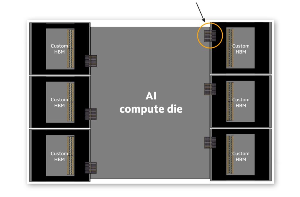
Marvell recently announced a new custom high-bandwidth memory (HBM) compute architecture that addresses the scaling challenges of XPUs in AI workloads. The new architecture enables higher compute and memory density, reduced power consumption, and lower TCO for custom XPUs.
Custom HBM for Cloud AI
Marvell’s custom high-bandwidth memory uses a new advanced architecture that enhances the performance, efficiency, and scalability of XPUs (eXtended Processing Units). It focuses on tailoring the memory subsystem to meet the unique demands of modern AI workloads.
Marvell is partnering with leading memory manufacturers Micron, Samsung Electronics, and SK hynix, to co-develop these custom HBM solutions.
Key Features
- Tailored Interfaces:
- Custom interfaces between HBM stacks and XPU compute dies optimize power, performance, and die size.
- Reduce power consumption of the interface by up to 70% compared to standard HBM solutions.
- Increased Memory Density:
- Supports up to 33% more HBM stacks per XPU, significantly boosting memory capacity.
- Achieves higher memory integration using advanced 2.5D packaging technology.
- Efficient Silicon Utilization:
- Reclaims up to 25% of silicon real estate by consolidating HBM support logic onto the base die.
- The saved space can be used to add compute logic, enhance features, or improve chip capabilities.
- Customizable Design:
- Adapts to specific workloads, enabling optimization for AI training, inference, or other application types.
- Tailors the memory subsystem, including the base die, HBM stack, and interfaces, for targeted performance, power, and cost metrics.
- Advanced Packaging:
- Uses high-speed industry-standard interfaces with advanced 2.5D packaging to enable faster data communication and reduce latency.
Background: What is HBM?
High-Bandwidth Memory is an advanced type of DRAM designed to provide high-speed data transfer rates and increased memory density. Unlike traditional DRAM, which typically resides on a separate module or chip, HBM is vertically stacked and integrated closely with processors (such as GPUs, CPUs, and XPUs) through advanced packaging techniques.
Key Characteristics of HBM
- Vertical Stacking:
- HBM uses a 3D architecture where multiple DRAM dies are stacked vertically on each other.
- The stacked dies are connected using Through-Silicon Vias (TSVs) — vertical electrical connections passing through the silicon.
- Close Integration with Processors:
- HBM stacks are integrated with processors via a high-speed interface located on a base die, often called the HBM base die.
- This proximity minimizes latency and increases the bandwidth between memory and processor.
- Advanced Packaging:
- HBM is packaged using 2.5D packaging technology, where the processor and memory stacks are mounted on an interposer—a silicon substrate that provides high-density interconnections.
- High Bandwidth:
- HBM delivers significantly higher bandwidth than conventional memory (e.g., DDR4 or GDDR), enabling rapid data transfer essential for compute-intensive tasks.
- Lower Power Consumption:
- HBM achieves high bandwidth with lower energy per bit transferred, making it more power-efficient than alternatives like GDDR.
Advantages of HBM
- High Performance: Offers bandwidths up to terabytes per second, making it suitable for demanding workloads such as AI training, gaming, and high-performance computing (HPC).
- Compact Form Factor: The stacked design reduces the memory’s footprint, saving space on the processor package.
- Energy Efficiency: Consumes less power for data transfer compared to traditional memory solutions.
Applications of HBM
- AI and Machine Learning: Provides the bandwidth needed for training large-scale neural networks and performing inference at scale.
- GPUs: Powers high-performance GPUs used in gaming, rendering, and visualization.
- Data Center Accelerators: Supports memory-intensive workloads in cloud computing and hyperscale environments.
- HPC Systems: Delivers the computational and memory performance required for scientific simulations and complex modeling.
HBM Generations
HBM has evolved through several generations, each improving capacity, bandwidth, and efficiency:
- HBM1: The first generation, offering up to 128GB/s per stack.
- HBM2 and HBM2E: Enhanced versions with increased capacity (up to 24GB per stack) and higher bandwidth.
- HBM3 and Beyond: Introduces even higher memory capacity and bandwidth, catering to next-generation AI and HPC demands.
Analysis
Traditional HBM designs face scaling challenges due to power and space requirements. Marvell’s custom approach mitigates these issues and aligns with the broader trend of custom silicon as a solution to Moore’s Law limitations.
Marvell’s new custom HBM solution helps solidify the company as a leader in the custom silicon market, where Marvell continues to execute extremely well. Marvell recently expanded its ongoing relationship with Amazon Web Services, where the company works with AWS on the design of its Trainium2 accelerator and provides other IP blocks for AWS’s Nitro system.
Marvell also works with another unnamed tier-one hyper-scaler (widely believed to be Google) on an internal ARM-based processor.
In its most recent earnings, Marvell noted that it grew its datacenter business a staggering 98% year-over-year to $1.1 billion in revenue. This growth was primarily driven by strong demand for its custom AI silicon solutions and Ethernet switch products. The new custom HBM will undoubtedly keep that demand alive moving forward.


